General Description
The RT8577A is an 4-CH LED driver capable of delivering 200mA for each channel. The RT8577A is a current mode boost converter with an adjustable switching frequency via the RT pin from 200kHz to 2.1MHz and a wide VIN range from 5V to 40V.
Performance Specification Summary
Summary of the RT8577A Evaluation Board performance specification is provided in Table 1. The ambient temperature is -40°C to 85°C.
Table 1. RT8577AGQW Evaluation Board Performance Specification Summary
|
Specification
|
Test Conditions
|
Min
|
Typ
|
Max
|
Unit
|
|
Input Voltage Range
|
|
5.5
|
--
|
40
|
V
|
|
LED1 to LED4 Regulation Voltage
|
ILED = 80mA
|
0.75
|
0.86
|
1
|
V
|
|
Switching Frequency
|
RRT = 20kΩ
|
1.8
|
2.1
|
2.4
|
MHz
|
|
RRT = Open
|
50
|
200
|
250
|
kHz
|
|
LED Current Accuracy
|
RISET = 15kΩ, VPWM > 1.2V
|
76
|
80
|
84
|
mA
|
|
LED Current Matching
|
ILED = 80mA

|
--
|
±1.5
|
±3
|
%
|
|
Maximum Duty Cycle
|
|
80
|
--
|
100
|
%
|
|
SEN Current Sense Limit
|
|
0.1
|
0.5
|
0.6
|
V
|
|
OVP Threshold
|
|
1.9
|
2
|
2.1
|
V
|
|
SCP Threshold
|
PWM freq = 2 kHz to 4kHz
|
6
|
7
|
8
|
V
|
Power-up Procedure
Suggestion Required Equipments
- RT8577A Evaluation Board
- DC power supply capable of at least 12V and 10A
- LED Load Board
- Function Generator
- Oscilloscope
Quick Start Procedures
The Evaluation Board is fully assembled and tested. Follow the steps below to verify board operation. Do not turn on supplies until all connections are made. When measuring the output voltage ripple, care must be taken to avoid a long ground lead on the oscilloscope probe. Measure the output voltage ripple by touching the probe tip and ground ring directly across the last output capacitor.
Proper measurement equipment setup and follow the procedure below.
1) With power off, connect the power supply for VIN and GND pins.
2) With power off, use jumper to pull high for EN pin.
3) With power off, connect the Function Generator to PWM pin.
4) With power off, connect the LED Load Board to VOUT and LEDx pins.
5) Turn on the power supply at the input. Make sure that the input voltage does not exceeds 24V on the Evaluation Board.
6) Turn on the Function Generator at the PWM pin.
7) Check LED Load Board brightness.
8) Once the proper output voltage is established, adjust the PWM duty within the operating ranges and observe the output LED brightness , ILEDx , efficiency and other performance.
Detailed Description of Hardware
Headers Description and Placement
Carefully inspect all the components used in the EVB according to the following Bill of Materials table, and then make sure all the components are undamaged and correctly installed. If there is any missing or damaged component, which may occur during transportation, please contact our distributors or e-mail us at evb_service@richtek.com.
Test Points
The EVB is provided with the test points and pin names listed in the table below.
|
Test Point/
Pin Name
|
Comment (expected waveforms or voltage levels on test points)
|
|
VIN
|
Power input. Support 5.5V to 40V Input Voltage. Must bypass with a suitable large ceramic capacitor at this pin.
|
|
EN
|
High = Enable. Apply an external clock to adjust the switching frequency.
|
|
GND
|
Ground.
|
|
Vout
|
Bootstrap supply for high-side gate driver. Connect a 0.1µF ceramic capacitor between the Vout and LX pins.
|
|
LX
|
Connect this pin to an external L-C filter.
|
|
LED4
|
Current sink for LED4.
|
|
LED3
|
Current sink for LED3.
|
|
LED2
|
Current sink for LED2.
|
|
LED1
|
Current sink for LED1.
|
Bill of Materials
|
VIN = 12V, VOUT = LED Load Board , IOUT = 80mA
|
|
Reference
|
Count
|
Part Number
|
Value
|
Description
|
Package
|
Manufacturer
|
|
U4
|
1
|
RT8577AGQW
|
RT8577A
|
LED Driver
|
WQFN-20L 5x5
|
RICHTEK
|
|
C19, C20, C21
|
3
|
1206B105K500CT
|
1µF
|
Capacitor, Ceramic
50V/X7R
|
1206
|
WALSIN
|
|
C22
|
1
|
0603B224K250CT
|
0.22μF
|
Capacitor, Ceramic
50V/X7R
|
0603
|
WALSIN
|
|
C24, C34
|
2
|
GRM32ER71H106KA12L
|
10µF
|
Capacitor, Ceramic
50V/X7R
|
1210
|
muRata
|
|
C25, C26, C27, C28, C30, C32
|
6
|
UMK316AB7475KL-T
|
4.7µF
|
Capacitor, Ceramic
50V/X7R
|
1206
|
TAIYO YUDEN
|
|
C29
|
1
|
LHK221M50V1015
|
220µF
|
Capacitor, Ceramic
50V
|
EC-2P/10
|
JACKCON
|
|
C33
|
1
|
0603B121K500CT
|
120pF
|
Capacitor, Ceramic
50V/X7R
|
0603
|
WALSIN
|
|
D2
|
1
|
SR26
|
2A/60V
|
Schottky Diode
|
SMA
|
PANJIT
|
|
L4
|
1
|
NR8040T150M
|
15µH
|
Power Inductor
|
L-D12_5
|
TAIYO YUDEN
|
|
Q5
|
1
|
DMN10H170SK3-13
|
59A/60V
|
MOSFET
|
TO-252
|
DIODES
|
|
R19
|
1
|
CR2512FR100E04Z
|
150mR
|
Resistor
|
2512
|
EVER OHMS
|
|
R22, R25, R40
|
3
|
WR06X1003FTL
|
100k
|
Resistor
|
0603
|
WALSIN
|
|
R23
|
1
|
WR06W1804FTL
|
1.8M
|
Resistor
|
0603
|
WALSIN
|
|
R24
|
1
|
WR08X10R0FTL
|
10R
|
Resistor
|
CP-0805C
|
WALSIN
|
|
R28
|
1
|
WR06X5600FTL
|
560R
|
Resistor
|
0603
|
WALSIN
|
|
R29
|
1
|
WR06W5R10FTL
|
5.1R
|
Resistor
|
0603
|
WALSIN
|
|
R30
|
1
|
RTT032002FTP
|
20k
|
Resistor
|
0603
|
WALSIN
|
|
R31
|
1
|
WR06X1000FTL
|
100R
|
Resistor
|
0603
|
WALSIN
|
|
R33
|
1
|
WR06X1802FTL
|
18k
|
Resistor
|
0603
|
WALSIN
|
|
R34
|
1
|
WR06X000 PTL
|
0R
|
Resistor
|
0603
|
WALSIN
|
|
R35, R37
|
2
|
WR06X5103FTL
|
510k
|
Resistor
|
0603
|
WALSIN
|
|
R36
|
1
|
WR06X1103FTL
|
110k
|
Resistor
|
0603
|
WALSIN
|
|
R39, R42
|
2
|
WR06X1001FTL
|
1k
|
Resistor
|
0603
|
WALSIN
|
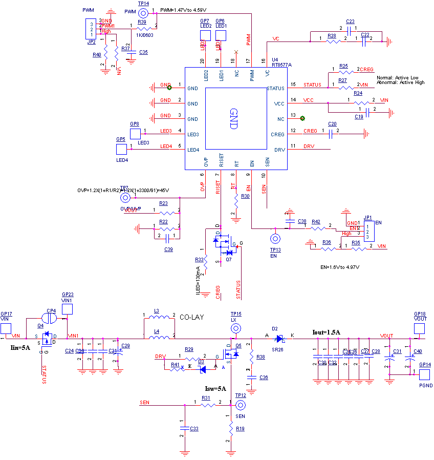
Typical Applications
EVB Schematic Diagram
1. The capacitance values of the input and output capacitors will influence the input and output voltage ripple.
2. MLCC capacitors have degrading capacitance at DC bias voltage, and especially smaller size MLCC capacitors will have much lower capacitance.
Measure Result
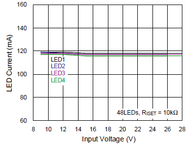
|
LED Current vs. Input Voltage
|
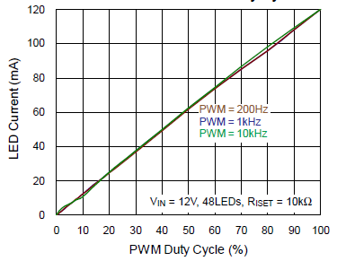
LED Current vs. PWM Duty Cycle
|
|
|
|
|
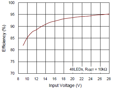
Efficiency vs. Input Voltage
|
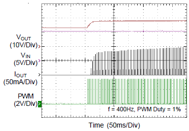
Start up with Minimum PWM Duty
|
|
|
|
|
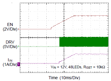
Power On from EN
|
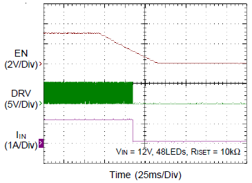
Power Off from EN
|
|
|
|
Evaluation Board Layout
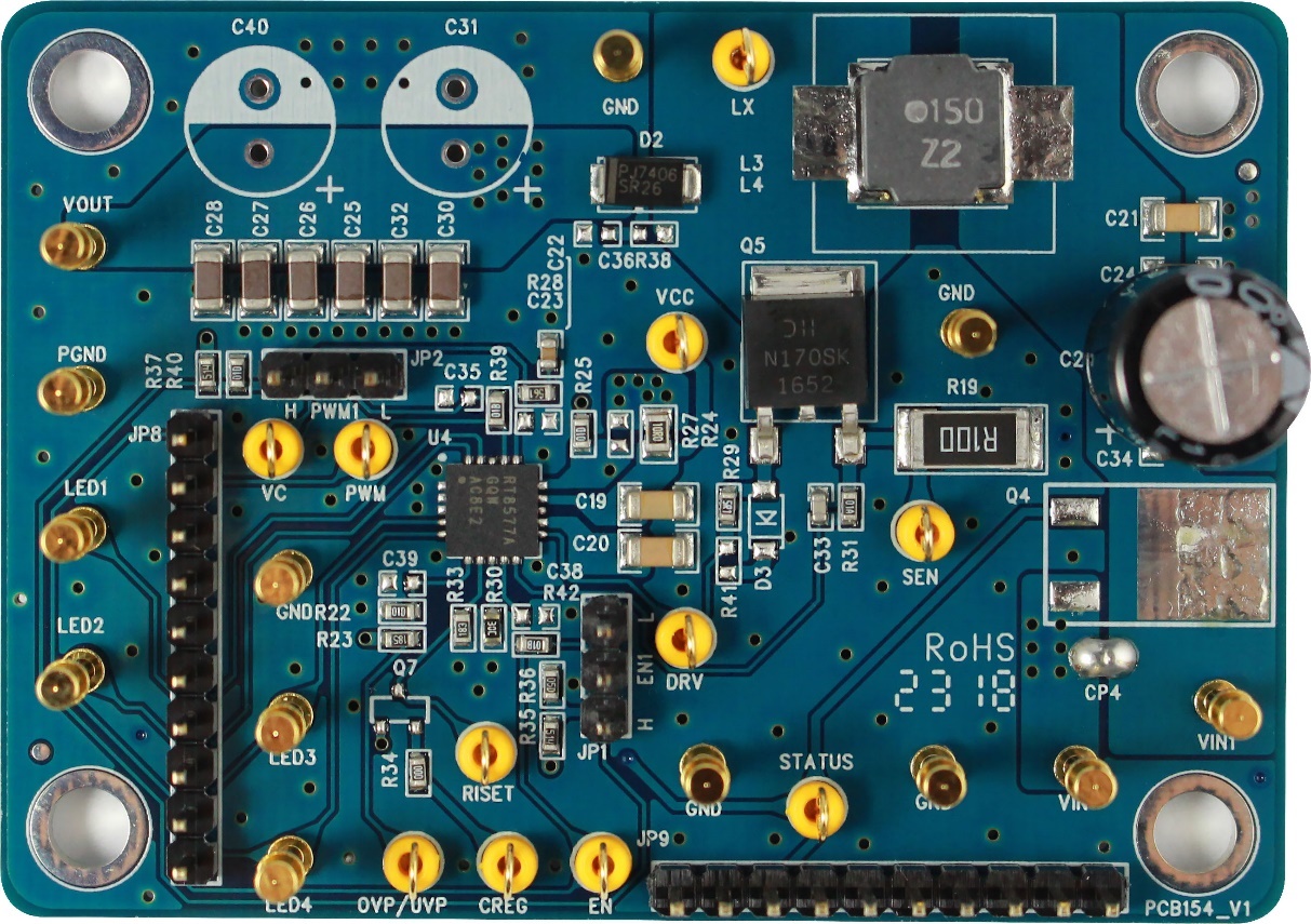
Figure 1 to Figure 4 are RT8577A Evaluation Board layout. This board size is 70mm x 50mm and is constructed on four-layer PCB, outer layers with 2 oz. Cu and inner layers with 1 oz. Cu.
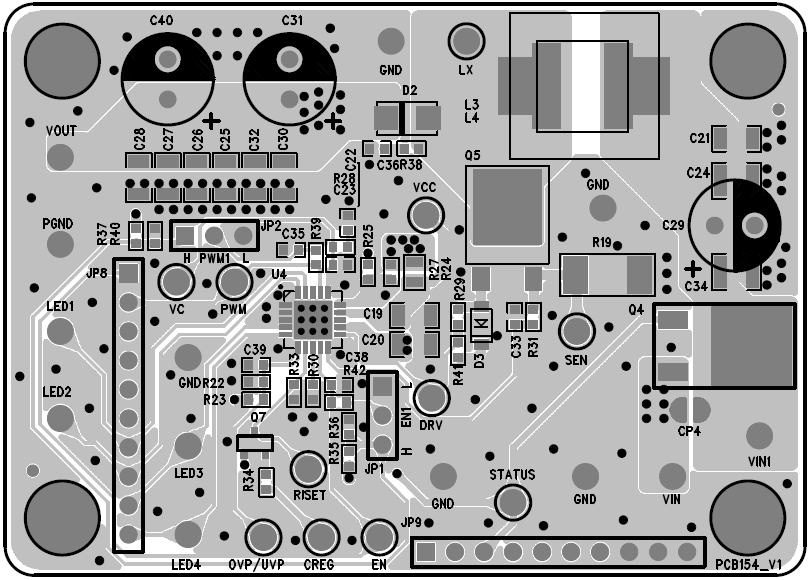
Figure 1. Top View (1st layer)
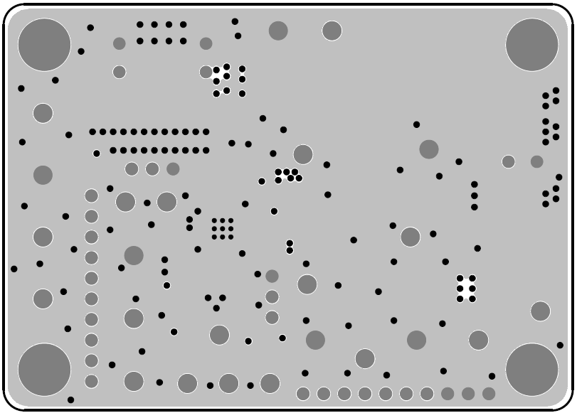
Figure 2. PCB Layout—Inner Side (2nd Layer)
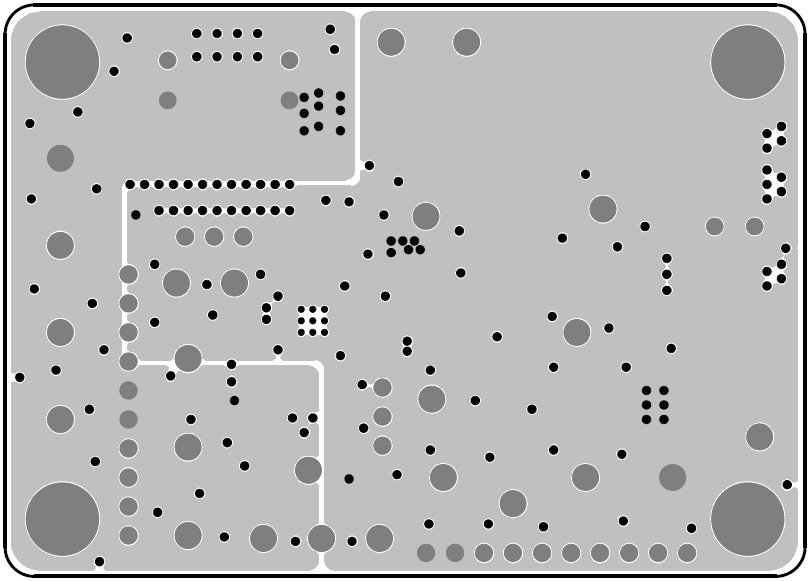
Figure 3. PCB Layout—Inner Side (3rd Layer)
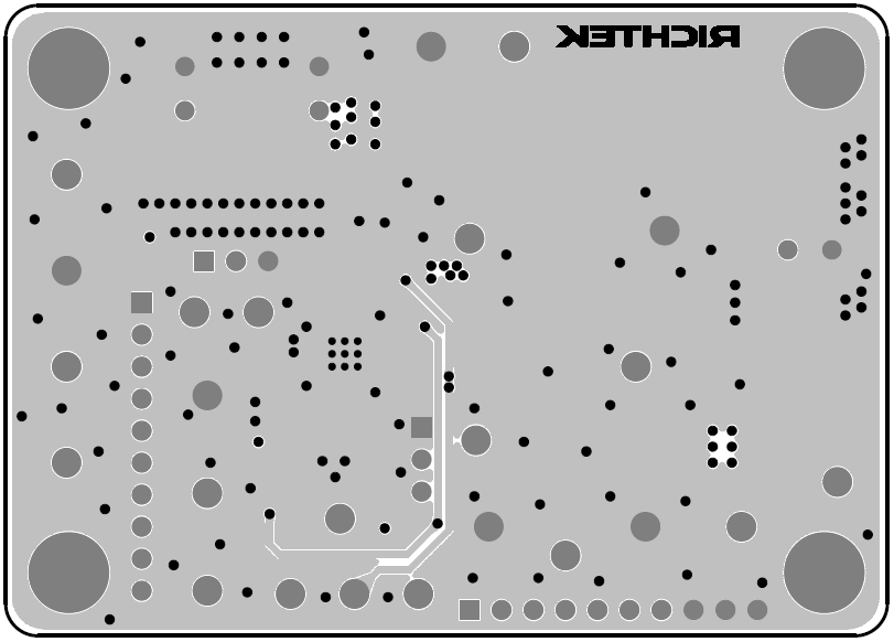
Figure 4. Bottom View (4th Layer)